
Design and simulation of a 4-bit CMOS shift register using 90 nm technology
Course: Microelectronics
Design and simulation of a 4-bit CMOS shift register using Synopsys Custom Compiler and the SAED 90 nm process design kit. The project followed a hierarchical integrated-circuit design methodology, progressing from transistor-level building blocks to the complete sequential circuit. CMOS inverters and transmission gates were used to implement 2-to-1 multiplexers and master-slave D flip-flops. Four flip-flop stages were then integrated to construct the complete 4-bit shift register. Transient simulations and test benches were used to verify signal propagation and data storage, while physical layouts were developed following the design rules of the 90 nm technology. 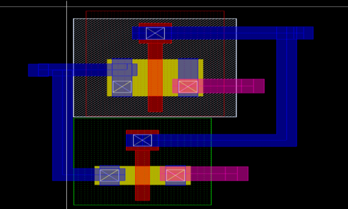
Design and Simulation
CMOS Inverter Physical Layout
Physical layout of the CMOS inverter implemented using the SAED 90 nm technology, including the PMOS and NMOS devices and their corresponding interconnections.
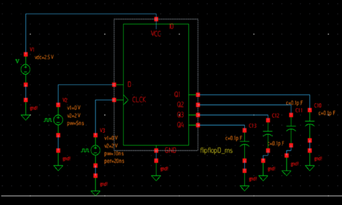
Simulation Test Bench
Test bench developed to validate the shift register under controlled clock and input signals and observe the behavior of its four outputs.
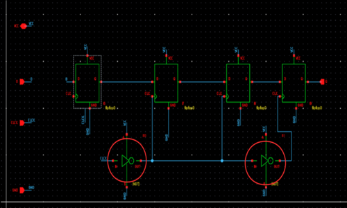
4-bit Shift Register Schematic
Hierarchical implementation of the 4-bit shift register using four D flip-flop stages connected to a common clock signal.
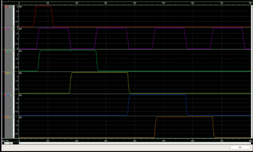
Transient Simulation
Transient simulation used to evaluate the propagation of the input data through the four sequential stages of the shift register.